

基本信息:
- 专利标题: REMOVABLE STRUCTURE AND REMOVAL METHOD USING THE STRUCTURE
- 申请号:US16969346 申请日:2019-01-14
- 公开(公告)号:US20210050249A1 公开(公告)日:2021-02-18
- 发明人: Didier Landru , Oleg Kononchuk , Nadia Ben Mohamed , Rénald Guerin , Norbert Colombet
- 申请人: Soitec
- 申请人地址: FR Bernin
- 专利权人: Soitec
- 当前专利权人: Soitec
- 当前专利权人地址: FR Bernin
- 优先权: FR1851179 20180213
- 国际申请: PCT/FR2019/050065 WO 20190114
- 主分类号: H01L21/762
- IPC分类号: H01L21/762
摘要:
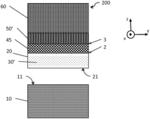
A detachable structure comprises a carrier substrate and a silicon oxide layer positioned on the substrate at a first interface. The detachable structure is notable in that: the oxide layer has a thickness of less than 200 nm; light hydrogen and/or helium species are distributed deeply and over the entire area of the structure according to an implantation profile, a maximum concentration of which is located in the thickness of the oxide layer; the total dose of implanted light species, relative to the thickness of the oxide layer, exceeds, at least by a factor of five, the solubility limit of these light species in the oxide layer.
公开/授权文献:
- US11424156B2 Removable structure and removal method using the structure 公开/授权日:2022-08-23
IPC结构图谱:
| H | 电学 |
| --H01 | 基本电气元件 |
| ----H01L | 半导体器件;其他类目未包含的电固体器件 |
| ------H01L21/00 | 专门适用于制造或处理半导体或固体器件或其部件的方法或设备 |
| --------H01L21/67 | .专门适用于在制造或处理过程中处理半导体或电固体器件的装置;专门适合于在半导体或电固体器件或部件的制造或处理过程中处理晶片的装置 |
| ----------H01L21/71 | ..限定在组H01L21/70中的器件的特殊部件的制造 |
| ------------H01L21/76 | ...组件间隔离区的制作 |
| --------------H01L21/762 | ....介电区 |