

基本信息:
- 专利标题: ELEMENT CHIP AND METHOD FOR MANUFACTURING THE SAME
- 申请号:US15427548 申请日:2017-02-08
- 公开(公告)号:US20170263526A1 公开(公告)日:2017-09-14
- 发明人: BUNZI MIZUNO , MITSURU HIROSHIMA , SHOGO OKITA , NORIYUKI MATSUBARA , ATSUSHI HARIKAI
- 申请人: Panasonic Intellectual Property Management Co., Ltd.
- 优先权: JP2016-048006 20160311
- 主分类号: H01L23/31
- IPC分类号: H01L23/31 ; H01L21/78 ; H01L21/428 ; H01L21/56 ; H01L21/311 ; H01L23/544
摘要:
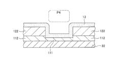
A method for manufacturing an element chip includes a protection film etching step of removing a part of the protection film which is stacked on the dividing region and the protection film which is stacked on the element region through etching the protection film anisotropically by exposing the substrate to first plasma and remaining the protection film for covering an end surface of the element region. Furthermore, the method for manufacturing an element chip includes an isotropic etching step of etching the dividing region isotropically by exposing the substrate to second plasma and a plasma dicing step of dividing the substrate to a plurality of element chips including the element region by exposing the substrate to third plasma in a state where the second main surface is supported by a supporting member.
公开/授权文献:
- US09911677B2 Element chip and method for manufacturing the same 公开/授权日:2018-03-06
IPC结构图谱:
| H | 电学 |
| --H01 | 基本电气元件 |
| ----H01L | 半导体器件;其他类目未包含的电固体器件 |
| ------H01L23/00 | 半导体或其他固态器件的零部件 |
| --------H01L23/02 | .容器;封接 |
| ----------H01L23/31 | ..按配置特点进行区分的 |