

基本信息:
- 专利标题: Semiconductor Device and Method of Manufacturing the Same
- 专利标题(中):半导体器件及其制造方法
- 申请号:US14162859 申请日:2014-01-24
- 公开(公告)号:US20140203357A1 公开(公告)日:2014-07-24
- 发明人: Daeik KIM , Jiyoung KIM , Jemin PARK , Nakjin SON , Yoosang HWANG
- 申请人: Daeik KIM , Jiyoung KIM , Jemin PARK , Nakjin SON , Yoosang HWANG
- 优先权: KR10-2013-0008125 20130124
- 主分类号: H01L29/423
- IPC分类号: H01L29/423 ; H01L29/78
摘要:
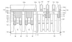
According to a method of manufacturing a semiconductor device, hard mask lines are formed in parallel in a substrate and the substrate between the hard mask lines is etched to form grooves. A portion of the hard mask line and a portion of the substrate between the grooves are etched. A top surface of the etched portion of the substrate between the grooves is higher than a bottom surface of the groove. A conductive layer is formed to fill the grooves. The conductive layer is etched to form conductive patterns in the grooves, respectively.
摘要(中):
根据半导体装置的制造方法,在基板上平行地形成硬掩模线,并且蚀刻硬掩模线之间的基板以形成凹槽。 硬掩模线的一部分和凹槽之间的基板的一部分被蚀刻。 在槽之间的衬底的蚀刻部分的顶表面高于槽的底表面。 形成导电层以填充凹槽。 蚀刻导电层以分别在凹槽中形成导电图案。
公开/授权文献:
- US09679982B2 Semiconductor device and method of manufacturing the same 公开/授权日:2017-06-13
IPC结构图谱:
| H | 电学 |
| --H01 | 基本电气元件 |
| ----H01L | 半导体器件;其他类目未包含的电固体器件 |
| ------H01L29/00 | 专门适用于整流、放大、振荡或切换,并具有至少一个电位跃变势垒或表面势垒的半导体器件;具有至少一个电位跃变势垒或表面势垒,例如PN结耗尽层或载流子集结层的电容器或电阻器;半导体本体或其电极的零部件 |
| --------H01L29/02 | .按其半导体本体的特征区分的 |
| ----------H01L29/41 | ..以其形状、相对尺寸或位置为特征的 |
| ------------H01L29/423 | ...不通有待整流、放大或切换电流的 |