

US12142564B2 Backside power distribution network semiconductor package and method of manufacturing the same
有权
基本信息:
- 专利标题: Backside power distribution network semiconductor package and method of manufacturing the same
- 申请号:US18457000 申请日:2023-08-28
- 公开(公告)号:US12142564B2 公开(公告)日:2024-11-12
- 发明人: Saehan Park , Hoonseok Seo , Jeonghyuk Yim , Ki-Il Kim , Gil Hwan Son
- 申请人: SAMSUNG ELECTRONICS CO., LTD.
- 申请人地址: KR Suwon-si
- 专利权人: SAMSUNG ELECTRONICS CO., LTD.
- 当前专利权人: SAMSUNG ELECTRONICS CO., LTD.
- 当前专利权人地址: KR Suwon-si
- 代理机构: Sughrue Mion, PLLC
- 分案原申请号: US17159972 2021.01.27
- 主分类号: H01L23/528
- IPC分类号: H01L23/528 ; H01L21/768 ; H01L21/822 ; H01L23/00 ; H01L23/48 ; H01L27/06
摘要:
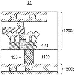
Provided is a semiconductor architecture including a carrier substrate, a landing pad included in the carrier substrate, a first semiconductor device provided on a first surface of the carrier substrate, the first semiconductor device including a first component provided on the landing pad, and a second semiconductor device provided on a second surface of the carrier substrate, a second component protruding from the second semiconductor device being provided on the landing pad.
公开/授权文献:
信息查询:
EspacenetIPC结构图谱:
| H | 电学 |
| --H01 | 基本电气元件 |
| ----H01L | 半导体器件;其他类目未包含的电固体器件 |
| ------H01L23/00 | 半导体或其他固态器件的零部件 |
| --------H01L23/34 | .冷却装置;加热装置;通风装置或温度补偿装置 |
| ----------H01L23/522 | ..包含制作在半导体本体上的多层导电的和绝缘的结构的外引互连装置的 |
| ------------H01L23/528 | ...互连结构的布置 |