

US10490568B2 Three-dimensional memory device with self-aligned drain side select gate electrodes and method of making thereof
有权
基本信息:
- 专利标题: Three-dimensional memory device with self-aligned drain side select gate electrodes and method of making thereof
- 申请号:US15927688 申请日:2018-03-21
- 公开(公告)号:US10490568B2 公开(公告)日:2019-11-26
- 发明人: James Kai , Murshed Chowdhury , Jin Liu , Johann Alsmeier
- 申请人: SANDISK TECHNOLOGIES LLC
- 申请人地址: US TX Plano
- 专利权人: SANDISK TECHNOLOGIES LLC
- 当前专利权人: SANDISK TECHNOLOGIES LLC
- 当前专利权人地址: US TX Addison
- 代理机构: The Marbury Law Group PLLC
- 主分类号: H01L27/11582
- IPC分类号: H01L27/11582 ; H01L27/11519 ; H01L27/11565 ; H01L27/11524 ; H01L27/1157 ; H01L27/11556 ; H01L29/423 ; H01L29/417 ; H01L29/51 ; H01L21/02 ; H01L21/311 ; H01L21/768
摘要:
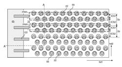
A three-dimensional memory device including self-aligned drain select level electrodes is provided. Memory stack structures extend through an alternating stack of insulating layers and spacer material layers. Each of the memory stack structures includes a memory film and a memory level channel portion. Drain select level channel portions are formed over the memory level channel portions with respective lateral shifts with respect to underlying memory stack structures. The direction of lateral shifts alternates from row to row for each row of drain select level channel portions. Drain select level gate dielectrics and drain select level gate electrodes are formed on the drain select level channel portions. Each drain select level gate electrode controls two rows of drain select level channel portions, and is laterally spaced from neighboring drain select level gate electrodes.
公开/授权文献:
信息查询:
EspacenetIPC结构图谱:
| H | 电学 |
| --H01 | 基本电气元件 |
| ----H01L | 半导体器件;其他类目未包含的电固体器件 |
| ------H01L27/00 | 由在一个共用衬底内或其上形成的多个半导体或其他固态组件组成的器件 |
| --------H01L27/02 | .包括有专门适用于整流、振荡、放大或切换的半导体组件并且至少有一个电位跃变势垒或者表面势垒的;包括至少有一个跃变势垒或者表面势垒的无源集成电路单元的 |
| ----------H01L27/04 | ..其衬底为半导体的 |
| ------------H01L27/06 | ...在非重复结构中包括有多个单个组件的 |
| --------------H01L27/105 | ....包含场效应组件的 |
| ----------------H01L27/112 | .....只读存储器结构的 |
| ------------------H01L27/115 | ......电动编程只读存储器 |
| --------------------H01L27/11502 | .......具有铁电体存储器电容器的 |
| ----------------------H01L27/11578 | ........以三维布置为特征的,例如,单元胞在不同的高度层 |
| ------------------------H01L27/1158 | .........具有在不同层的源区和漏区的,例如,具有倾斜沟道的 |
| --------------------------H01L27/11582 | ..........沟道具有垂直部分的,例如,U形沟道 |